Luận án tiến sĩ kỹ thuật hóa học green and low cost preparation of cigse thin fi
Tài liệu: Luận án tiến sĩ kỹ thuật hóa học green and low cost preparation of cigse thin film by a nanocrystals ink based spin coating method. Tải miễn phí tại T
Yeungnam University
Luan An
Luận án tiến sĩ
Năm xuất bản
Số trang
81
Thời gian đọc
13 phút
Lượt xem
2
Lượt tải
0
Phí lưu trữ
40 Point
Tổng quan nhanh
- Chủ đề:
- 1. Phương pháp Điều chế Màng mỏng CIGSe Xanh và Chi phí Thấp
- Số trang:
- 81 trang
- Trường:
- Yeungnam University
- Chuyên ngành:
- Chemical Engineering
- Tác giả:
- Le Thi Thuy Trang
- Năm:
- 2020
Tóm tắt nội dung luận án
I. Phương pháp Điều chế Màng mỏng CIGSe Xanh và Chi phí Thấp
Nghiên cứu này trình bày một quy trình sáng tạo. Mục tiêu là sản xuất màng mỏng CIGSe chất lượng cao. Phương pháp này đặc biệt chú trọng tính bền vững và hiệu quả kinh tế. Các phương pháp sản xuất truyền thống cho vật liệu hấp thụ CIGSe thường tốn kém. Chúng cũng yêu cầu môi trường chân không phức tạp. Điều này hạn chế ứng dụng rộng rãi trong ngành pin mặt trời. Luận án giải quyết những thách thức này. Nó phát triển một quy trình tổng hợp hóa học bền vững và chi phí thấp. Quy trình này thân thiện môi trường, giảm thiểu chất thải. Nó mở ra triển vọng thương mại hóa pin mặt trời CIGSe hiệu quả hơn.
1.1. Tổng quan về Công nghệ Quang điện Màng mỏng CIGSe
CIGSe (Đồng-Indi-Gali-Selen) là vật liệu bán dẫn quan trọng. Nó được dùng làm lớp hấp thụ ánh sáng trong pin mặt trời màng mỏng. Vật liệu này có tiềm năng hiệu suất cao. Tuy nhiên, việc điều chế CIGSe thường phức tạp. Các phương pháp hiện có đòi hỏi chi phí đầu tư lớn. Chúng cũng tiêu thụ nhiều năng lượng. Nhu cầu về một quy trình sản xuất sạch hơn là cấp thiết. Nó cần giảm thiểu tác động đến môi trường. Đồng thời, nó cần đạt được chi phí thấp. Điều này sẽ thúc đẩy sự phát triển của vật liệu xanh và kỹ thuật xanh trong năng lượng tái tạo.
1.2. Giới thiệu Quy trình dựa trên Dung dịch Mực và Phủ quay
Luận án đề xuất một cách tiếp cận mới. Quy trình dựa trên dung dịch mực hạt nano CIGSe. Kỹ thuật phủ quay (spin-coating) được sử dụng để tạo màng. Sau đó, quá trình nhiệt luyện trong môi trường selen được thực hiện. Đây là một phương pháp điều chế chi phí thấp và thân thiện môi trường. Nó không yêu cầu chân không. Quy trình này thể hiện sự tiến bộ trong hóa học xanh. Nó hứa hẹn mang lại hiệu quả năng lượng cao. Đồng thời, nó đáp ứng tiêu chí tổng hợp hóa học bền vững. Quy trình này tối ưu hóa quy trình sản xuất màng CIGSe.
II. Tổng hợp Hạt nano CIGSe Xanh bằng Phương pháp Siêu âm
Tổng hợp hạt nano CIGSe là bước đầu tiên của quy trình. Một phương pháp sonochemical (siêu âm) đã được phát triển. Phương pháp này sử dụng dung môi xanh ethanol. Ethanol là một lựa chọn an toàn. Nó giúp giảm thiểu độc hại so với các dung môi truyền thống. Việc sử dụng siêu âm giúp tổng hợp hiệu quả. Nó không cần gia nhiệt bổ sung. Điều này giảm đáng kể chi phí năng lượng. Nó cũng góp phần vào mục tiêu giảm thiểu chất thải. Đây là một ví dụ điển hình về kỹ thuật xanh trong tổng hợp vật liệu. Luận án tập trung vào việc tạo ra các hạt nano chất lượng cao, đồng nhất.
2.1. Vai trò của Dung môi Xanh và Phương pháp Siêu âm
Hạt nano CIGSe được tổng hợp bằng phương pháp siêu âm. Dung môi ethanol chứa NaBH4 đóng vai trò quan trọng. Ethanol là dung môi xanh, không độc hại. Nó là lựa chọn lý tưởng cho một quy trình thân thiện môi trường. NaBH4 thúc đẩy phản ứng tổng hợp hiệu quả. Phương pháp siêu âm giúp phân tán năng lượng đồng đều. Nó tạo ra các hạt nano với hình thái học kiểm soát được. Không cần gia nhiệt thêm, quy trình này tiết kiệm năng lượng. Đây là một cách tiếp cận điều chế chi phí thấp và tổng hợp hóa học bền vững.
2.2. Tối ưu hóa Thời gian Siêu âm và Cấu trúc Hạt nano
Thời gian siêu âm là yếu tố then chốt. Luận án đã khảo sát các khoảng thời gian từ 2 đến 5 giờ. Thời gian 5 giờ được xác định là tối ưu. Nó tạo ra hạt nano CuIn0.7Ga0.3Se2 mong muốn. Các hạt nano CIGSe tổng hợp có cấu trúc tetragonal. Chúng có hình dạng gần như hình cầu, kích thước đồng đều. Công thức hóa học mục tiêu là Cu(In0.7Ga0.3)Se2. Một cơ chế phản ứng mới đã được đề xuất. Nó giải thích vai trò của NaBH4 trong quá trình. Việc tối ưu hóa quy trình sản xuất này đảm bảo chất lượng vật liệu đầu vào.
III. Tối ưu hóa Dung dịch Mực nano CIGSe và Lớp Phim hấp thụ
Sau khi tổng hợp, các hạt nano CIGSe được dùng để tạo dung dịch mực. Sự ổn định của dung dịch mực là cực kỳ quan trọng. Nó ảnh hưởng trực tiếp đến chất lượng màng mỏng cuối cùng. Nghiên cứu đã đánh giá ba loại dung môi khác nhau. Mục tiêu là tìm ra dung môi phân tán tốt nhất. Quy trình này hướng tới việc tạo ra một vật liệu xanh. Nó được sử dụng trong các quy trình sản xuất sạch hơn. Việc tối ưu hóa dung dịch mực là một bước thiết yếu. Nó đảm bảo độ đồng đều và độ bám dính của lớp phim. Điều này ảnh hưởng đến hiệu quả năng lượng của pin mặt trời.
3.1. Nghiên cứu Dung môi phân tán cho Mực nano CIGSe bền vững
Để tạo dung dịch mực ổn định, ba dung môi được thử nghiệm. Chúng bao gồm 2-propanol, 2-methoxyethanol và hỗn hợp 2:1 của chúng. Hỗn hợp 2-propanol : 2-methoxyethanol = 2 : 1 (v/v) cho kết quả tốt nhất. Nó tạo ra dung dịch mực ổn định cho hạt nano CIGSe. Dung dịch mực ổn định là nền tảng. Nó đảm bảo quá trình phủ quay diễn ra hiệu quả. Lựa chọn dung môi phù hợp là một phần của kỹ thuật xanh. Nó góp phần vào một quy trình thân thiện môi trường và giảm thiểu chất thải.
3.2. Tác động của Các chế độ Nhiệt luyện đến Cấu trúc Màng CIGSe
Các chế độ nhiệt luyện khác nhau được nghiên cứu. Chúng ảnh hưởng đến kích thước hạt và mật độ của màng CIGSe. Màng mỏng CIGSe thu được có độ dày khoảng 1 µm. Nó sở hữu cấu trúc tetragonal đặc trưng. Năng lượng vùng cấm ước tính khoảng ~1.2 eV. Đây là các thông số lý tưởng cho lớp hấp thụ pin mặt trời. Việc tối ưu hóa quy trình sản xuất nhiệt luyện rất quan trọng. Nó giúp nâng cao chất lượng vật liệu xanh. Nó đảm bảo hiệu suất hoạt động của thiết bị quang điện.
IV. Quy trình Sản xuất Không Chân không Hiệu quả và Tiềm năng
Quy trình không chân không mới đã được áp dụng thành công. Từ tổng hợp hạt nano đến tạo dung dịch mực. Sau đó là hình thành màng mỏng CIGSe chất lượng cao. Phương pháp này thể hiện tính ưu việt. Nó là một quy trình điều chế chi phí thấp. Nó cũng là một kỹ thuật xanh. Quy trình này mở ra một con đường mới. Con đường hướng tới thương mại hóa pin mặt trời CIGSe cạnh tranh. Nó giảm thiểu chất thải. Nó cũng nâng cao hiệu quả năng lượng. Quy trình này là bước tiến quan trọng trong sản xuất sạch hơn.
4.1. Ưu điểm của Quy trình Không Chân không và Chất lượng Màng
Quy trình không chân không mang lại nhiều lợi ích. Nó loại bỏ nhu cầu về thiết bị chân không đắt tiền và phức tạp. Điều này giúp giảm đáng kể chi phí sản xuất. Nó cũng là một quy trình thân thiện môi trường hơn. Màng mỏng CIGSe sản xuất bằng phương pháp này có chất lượng cao. Chúng có cấu trúc tinh thể tốt và tính chất quang điện mong muốn. Đây là minh chứng cho thành công của một phương pháp tổng hợp hóa học bền vững. Nó cũng thể hiện khả năng tối ưu hóa quy trình sản xuất hiệu quả.
4.2. Mở ra Con đường Thương mại hóa Pin mặt trời CIGSe cạnh tranh
Việc sản xuất màng CIGSe chất lượng cao với chi phí thấp là đột phá. Nó mở ra cơ hội thương mại hóa rộng rãi. Đặc biệt là cho pin mặt trời màng mỏng CIGSe. Quy trình này có tiềm năng thay đổi ngành công nghiệp. Nó giúp phát triển vật liệu xanh và sản xuất sạch hơn. Nó cung cấp một giải pháp năng lượng tái tạo bền vững. Đây là một bước tiến quan trọng. Nó giúp pin mặt trời CIGSe trở nên cạnh tranh hơn trên thị trường toàn cầu. Nó góp phần vào mục tiêu hiệu quả năng lượng và giảm thiểu chất thải.
Mục lục chi tiết luận án
Tải xuống file đầy đủ để xem toàn bộ nội dung
Tải đầy đủ (81 trang)Nội dung chính
Tổng quan về luận án
Sự bùng nổ của ngành năng lượng tái tạo đặt ra yêu cầu cấp thiết về việc phát triển các công nghệ quang điện (photovoltaic - PV) hiệu suất cao nhưng có chi phí sản xuất thấp và thân thiện với môi trường. Trong các vật liệu bán dẫn màng mỏng thế hệ thứ hai, hợp chất bán dẫn bốn thành phần $\text{Cu}(\text{In}{x}\text{Ga}{1-x})\text{Se}_2$ (CIGSe) thuộc họ chalcopyrite $\text{I-III-VI}_2$ nổi lên như một lớp hấp thụ ánh sáng (absorber layer) lý tưởng nhờ hệ số hấp thụ quang học vượt trội ($\alpha > 10^5 \text{ cm}^{-1}$) và vùng cấm trực tiếp (direct bandgap) có thể điều chỉnh linh hoạt từ $1.04\text{ eV}$ ($\text{CuInSe}_2$) đến $1.68\text{ eV}$ ($\text{CuGaSe}_2$). Mặc dù pin mặt trời CIGSe chế tạo bằng phương pháp đồng bốc bay nhiệt chân không cao (high-vacuum co-evaporation) ba giai đoạn đã đạt hiệu suất kỷ lục $23.35%$, quy trình này đòi hỏi môi trường chân không khắt khe ($10^{-6}\text{ torr}$ hoặc thấp hơn) và thiết bị đắt đỏ, làm gia tăng chi phí sản xuất công nghiệp và tiêu hao năng lượng.
Nghiên cứu của nghiên cứu sinh Lê Thị Thùy Trang dưới sự hướng dẫn của Giáo sư Chinho Park và đồng hướng dẫn của Giáo sư JaeHong Kim tại Khoa Kỹ thuật Hóa học, Trường Sau đại học Đại học Yeungnam (Yeungnam University, 2020) với tiêu đề "Green and low-cost preparation of CIGSe thin film by a nanocrystals ink based spin-coating method" đã mở ra bước đột phá trong việc chế tạo màng mỏng CIGSe thông qua quy trình phi chân không (non-vacuum) kết hợp hóa học siêu âm (sonochemical method) và phủ quay (spin-coating).
Khoảng trống nghiên cứu (research gap) trọng tâm mà luận án giải quyết là sự phụ thuộc của các phương pháp dung dịch truyền thống vào các dung môi độc hại cao như hydrazine ($\text{N}_2\text{H}_4$), ethylenediamine, polyetheramine hoặc trioctylphosphine (TOP), cũng như yêu cầu nhiệt độ phản ứng cao ($180 - 280^\circ\text{C}$) trong thiết bị chịu áp (autoclave/glove-box). Thậm chí, công trình nghiên cứu sonochemical trước đây của Cha và cộng sự (2013) vẫn phải sử dụng hỗn hợp hydrazine và ethylene glycol ở $110^\circ\text{C}$ do độ nhớt cao của dung môi ($\sim 16.1\text{ mPa}\cdot\text{s}$ ở $20^\circ\text{C}$) cản trở sự phát triển của bọt khí xâm thực. Luận án đặt ra hệ thống câu hỏi nghiên cứu và giả thuyết khoa học cụ thể:
- Câu hỏi nghiên cứu 1 (RQ1): Làm thế nào để tổng hợp pha tinh thể $\text{CuIn}{0.7}\text{Ga}{0.3}\text{Se}_2$ đơn pha ở nhiệt độ phòng mà không sử dụng dung môi độc hại hoặc chất hoạt hóa bề mặt hữu cơ (capping agents)?
- Câu hỏi nghiên cứu 2 (RQ2): Vai trò khử và hòa tan của $\text{NaBH}_4$ trong dung môi phân cực xanh ethanol diễn ra theo cơ chế phản ứng nào dưới tác động của trường siêu âm công suất cao?
- Câu hỏi nghiên cứu 3 (RQ3): Tỷ lệ phối trộn dung môi phân tán nào tối ưu hóa độ ổn định keo của mực hạt nano CIGSe và ngăn chặn hiện tượng kết tụ khi phủ quay màng mỏng?
- Giả thuyết 1 (H1): Dung môi ethanol với độ nhớt thấp ($\sim 1.2\text{ mPa}\cdot\text{s}$ ở $20^\circ\text{C}$) sẽ tối ưu hóa hiệu ứng xâm thực âm học (acoustic cavitation), tạo ra các điểm nóng cục bộ (localized hot spots) đủ năng lượng kích hoạt phản ứng phân hủy pha tạp $\text{Cu}2\text{Se}$ và chuyển hóa hoàn toàn thành cấu trúc tứ giác chalcopyrite $\text{CuIn}{0.7}\text{Ga}_{0.3}\text{Se}_2$ khi kéo dài thời gian siêu âm lên 5 giờ.
- Giả thuyết 2 (H2): Hệ dung môi phân tán nhị phân giữa 2-propanol và 2-methoxyethanol theo tỷ lệ thể tích $2:1\text{ (v/v)}$ sẽ tạo ra độ phân tán keo bền vững trên 1 tháng, cho phép tạo màng CIGSe đặc khít, độ dày $\sim 1\text{ }\mu\text{m}$, cấu trúc tinh thể cao và vùng cấm quang học tối ưu sau khi ủ selen hóa.
Khung lý thuyết của nghiên cứu tích hợp lý thuyết xâm thực âm học (acoustic cavitation theory), định luật Vegard về thông số mạng tinh thể, lý thuyết vùng năng lượng chất bán dẫn (band theory of semiconductors) và phương trình quang sai thực nghiệm (optical bowing equation). Về mặt quy mô, nghiên cứu tiến hành khảo sát các mốc thời gian siêu âm ($2\text{ giờ}$, $3.5\text{ giờ}$, và $5\text{ giờ}$) với hệ siêu âm tần số $20\text{ kHz}$, công suất $300\text{ W}$, kiểm soát nhiệt độ tự sinh ở mức $61 - 64^\circ\text{C}$, phân tích màng mỏng dày xấp xỉ $1\text{ }\mu\text{m}$ với kích thước hạt nano ban đầu $8\text{ nm}$ và phát triển lên $17 - 30\text{ nm}$ sau xử lý nhiệt.
       [Precursors: CuCl, InCl3, Ga(NO3)3, Se, NaBH4 in Ethanol]
                                  │
                                  ▼
      [Sonochemical Synthesis: f = 20 kHz, P = 300 W, t = 5 hours]
                                  │
                                  ▼
         [Quasi-spherical CuIn0.7Ga0.3Se2 Nanoparticles (~8 nm)]
                                  │
                                  ▼
   [Nanocrystal Ink Formulation: 2-Propanol + 2-Methoxyethanol (2:1 v/v)]
                                  │
                                  ▼
       [Spin-Coating Deposition on Substrate (Film thickness ~1 µm)]
                                  │
                                  ▼
          [Post-Annealing / Selenization at 500°C in N2/Se ambient]
                                  │
                                  ▼
       [High-Quality Tetragonal Chalcopyrite Absorber Layer: Eg ~ 1.15 eV]
Literature Review và Positioning
Lịch sử phát triển của pin mặt trời bắt đầu từ khám phá hiệu ứng quang điện của nhà vật lý người Pháp Alexandre Edmond Becquerel năm 1839. Thế hệ pin mặt trời thứ nhất dựa trên phiến silic đơn tinh thể (mono c-Si) khởi đầu từ công trình của Chapin, Fuller và Pearson (1954) tại Bell Laboratories với hiệu suất $6%$, sau đó được Hoffman Electronics thương mại hóa ($2%$) và Mandelkorn ứng dụng trên vệ tinh Vanguard 1. Dù hiệu suất c-Si hiện nay đã vượt $26%$, quy trình làm sạch vật liệu khối tiêu tốn năng lượng khổng lồ.
Để khắc phục nhược điểm của thế hệ thứ nhất, pin mặt trời màng mỏng thế hệ thứ hai ra đời với độ dày lớp hấp thụ chỉ từ $1 - 4\text{ }\mu\text{m}$. Trong đó, màng mỏng CIGSe được phát triển qua hai nhánh kỹ thuật chính: kỹ thuật chân không và kỹ thuật phi chân không.
Trong kỹ thuật chân không, phương pháp đồng bốc bay (co-evaporation) tiến triển từ quy trình 1 giai đoạn (tạo màng giàu khuyết tật, hạt nhỏ $< 1\text{ }\mu\text{m}$) sang quy trình 2 giai đoạn của Mickelsen và Chen (1982, 1983) phát triển màng từ lớp tiền chất giàu Cu ở $400 - 450^\circ\text{C}$ sang lớp nghèo Cu ở $500 - 550^\circ\text{C}$ thông qua cơ chế hơi - lỏng - rắn (vapour-liquid-solid - VLS). Đỉnh cao là quy trình 3 giai đoạn của Kessler và cộng sự (1993), lắng đọng $(\text{In},\text{Ga})_x\text{Se}_y$ ở $330^\circ\text{C}$, sau đó đồng bốc bay Cu và Se ở $500 - 560^\circ\text{C}$ đạt tỷ lệ $\text{Cu}/(\text{In}+\text{Ga}) = 1.15$ để phát triển kích thước hạt, và cuối cùng bổ sung In, Ga, Se để đưa tỷ lệ màng về mức nghèo Cu $\text{Cu}/(\text{In}+\text{Ga}) \sim 0.85 - 0.9$. Bên cạnh đó, phương pháp phún xạ (sputtering) hai bước do Chu và cộng sự khởi xướng lắng đọng lớp kim loại rồi tiến hành selen hóa sau.
Đối với kỹ thuật phi chân không dựa trên hạt nano, các nghiên cứu quốc tế đã tiếp cận qua nhiều hướng:
- Phương pháp tiêm nóng (hot-injection) và gia nhiệt (heat-up): Tang và cộng sự (2010) sử dụng dung môi oleylamine ở $80^\circ\text{C}$ để tiêm dung dịch Se; Ahmadi và cộng sự (2012) dùng hexadecylamine; Li và cộng sự (2011) tổng hợp CISe trong dodecylthiol và trioctylphosphine (TOP); Singh và cộng sự (2014) tổng hợp quy mô lớn bằng dodecylamine. Nhược điểm chí mạng là các phối tử hữu cơ chuỗi dài bám dính trên bề mặt hạt nano cản trở quá trình truyền điện tích và tạo bọt xốp carbon khi ủ màng.
- Phương pháp thủy nhiệt (hydrothermal) và dung môi nhiệt (solvothermal): Chun và cộng sự (2009) tổng hợp CIGS ở $280^\circ\text{C}$ trong $36\text{ giờ}$; Gu và cộng sự (2006) thực hiện ở $230^\circ\text{C}$ trong $24\text{ giờ}$; Li và cộng sự (1999) sử dụng ethylenediamine ở $180^\circ\text{C}$ trong $15\text{ giờ}$; Wu và cộng sự (2011) tổng hợp ở $180^\circ\text{C}$ trong $1\text{ giờ}$. Các phương pháp này đòi hỏi autoclave áp suất cao và tiêu hao năng lượng lớn.
- Phương pháp polyol: Khởi xướng bởi Fievet và cộng sự (1980s), Palchik và cộng sự dùng triethylene glycol; Wu và cộng sự (2013) tổng hợp trong tetraethylene glycol ở $280^\circ\text{C}$.
- Phương pháp hóa học siêu âm (sonochemical): Cha và cộng sự (2013) tổng hợp CIGSe bằng siêu âm trong $4\text{ giờ}$ nhưng buộc phải dùng dung môi ethylene glycol pha hydrazine ở $110^\circ\text{C}$ và sản phẩm chỉ kết tinh chalcopyrite sau khi ủ $500^\circ\text{C}$. Ngược lại, Badgujar và cộng sự (2014) sử dụng selenourea trong môi trường nước nhưng độ tinh khiết pha và khả năng kiểm soát tỷ lệ thành phần còn hạn chế.
Bảng đối sánh vị thế học thuật giữa luận án và các công trình quốc tế tiêu biểu:
| Tiêu chí nghiên cứu | Nghiên cứu của Cha et al. (2013) | Nghiên cứu của Singh et al. (2014) | Luận án của Lê Thị Thùy Trang (2020) |
|---|---|---|---|
| Hệ dung môi tổng hợp | Ethylene glycol + Hydrazine | Dodecylamine (phối tử chuỗi dài) | Ethanol nguyên chất ($99.9%$) + $\text{NaBH}_4$ |
| Nhiệt độ phản ứng | $110^\circ\text{C}$ (gia nhiệt cưỡng bức) | $> 200^\circ\text{C}$ (gia nhiệt kiểm soát) | Nhiệt độ phòng ($61 - 64^\circ\text{C}$ do siêu âm) |
| Độ độc hại hóa chất | Cực cao (Hydrazine gây ung thư) | Trung bình (Dung môi hữu cơ) | Thấp (Dung môi xanh tái tạo) |
| Pha tinh thể sau tổng hợp | Vô định hình / pha trung gian | Chalcopyrite có bọc phối tử hữu cơ | Tứ giác Chalcopyrite đơn pha thuần khiết |
| Tạp chất thứ cấp | Xuất hiện pha nhị phân | Tồn dư carbon do ligand hữu cơ | Loại bỏ hoàn toàn $\text{Cu}_2\text{Se}$ ở mốc $5\text{ giờ}$ |
Vị thế nghiên cứu của luận án được khẳng định khi lần đầu tiên thiết lập một lộ trình "xanh hóa toàn diện" (green route): sử dụng ethanol làm dung môi duy nhất, loại bỏ hoàn toàn chất hoạt hóa bề mặt hữu cơ, không cần gia nhiệt ngoài, và thu được trực tiếp hạt nano chalcopyrite $\text{CuIn}{0.7}\text{Ga}{0.3}\text{Se}_2$ kích thước siêu mịn $\sim 8\text{ nm}$.
Đóng góp lý thuyết và khung phân tích
Đóng góp cho lý thuyết
Luận án mở rộng lý thuyết xâm thực âm học (acoustic cavitation) của Suslick trong lĩnh vực tổng hợp vật liệu bán dẫn đa nguyên tố phức tạp. Cơ chế hình thành bọt khí, giãn nở và sụp đổ bão hòa giải phóng nhiệt độ tức thời lên đến hàng ngàn Kelvin và áp suất hàng trăm megapascal tại các vi bọt cục bộ. Luận án chứng minh rằng độ nhớt dung môi đóng vai trò quyết định: ethanol với độ nhớt cực thấp ($\sim 1.2\text{ mPa}\cdot\text{s}$) cho phép các bọt khí xâm thực phát triển tới kích thước cực đại trước khi sụp đổ, cung cấp mật độ năng lượng cao hơn hẳn môi trường ethylene glycol ($\sim 16.1\text{ mPa}\cdot\text{s}$).
Mô hình lý thuyết động học 5 phản ứng kế tiếp được đề xuất và kiểm chứng thực nghiệm:
$$\text{Se} + \text{NaBH}_4 + 3\text{C}_2\text{H}_5\text{OH} \rightarrow \text{NaHSe} + (\text{C}_2\text{H}_5\text{O})_3\text{B} + 3\text{H}_2 \uparrow \quad (1)$$
$$4\text{Ga}^{3+} + 6\text{HSe}^- \rightarrow 2\text{Ga}_2\text{Se}_3 + 6\text{H}^+ \quad (2)$$
$$4\text{In}^{3+} + 6\text{HSe}^- \rightarrow 2\text{In}_2\text{Se}_3 + 6\text{H}^+ \quad (3)$$
$$2\text{Cu}^+ + \text{HSe}^- \xrightarrow{\text{ultrasonication}} \text{Cu}_2\text{Se} + \text{H}^+ \quad (4)$$
$$\text{Cu}_2\text{Se} + x\text{In}_2\text{Se}_3 + (1-x)\text{Ga}_2\text{Se}_3 \xrightarrow{\text{ultrasonication}} 2\text{CuIn}x\text{Ga}{1-x}\text{Se}_2 \quad (5)$$
Cơ chế này giải thích chính xác sự biến đổi pha: ở thời gian siêu âm $2\text{ giờ}$, năng lượng chưa đủ để hoàn tất chuỗi phản ứng; ở $3.5\text{ giờ}$, xuất hiện pha chalcopyrite nhưng vẫn còn tồn dư $\text{Cu}_2\text{Se}$; chỉ khi đạt $5\text{ giờ}$ siêu âm, sóng âm kích thích phân hủy triệt để trung gian $\text{Cu}_2\text{Se}$ phản ứng với $\text{In}_2\text{Se}_3$ và $\text{Ga}_2\text{Se}_3$, tạo nên mạng tinh thể tứ giác đồng nhất.
Nghiên cứu cũng đóng góp vào việc kiểm chứng định luật Vegard trên vật liệu nano chalcopyrite bốn thành phần. Định luật Vegard biểu diễn mối quan hệ tuyến tính giữa hằng số mạng và tỷ lệ hợp phần:
$$a_{\text{CuIn}x\text{Ga}{1-x}\text{Se}2} = x \cdot a{\text{CuInSe}2} + (1-x) \cdot a{\text{CuGaSe}_2} \quad (6)$$
Dựa trên dữ liệu nhiễu xạ tia X (XRD) chuẩn JCPDS 03-065-4869 ($a = b = 5.7820\text{ \AA}$, $c = 11.6200\text{ \AA}$ cho $\text{CuInSe}2$) và các giá trị tính toán cho $\text{CuIn}{0.7}\text{Ga}{0.3}\text{Se}2$ ($a = b = 5.6960\text{ \AA}$, $c = 11.4480\text{ \AA}$), kết quả thực nghiệm của hạt nano tổng hợp ở mốc 5 giờ đạt $a = b = 5.6880\text{ \AA}$, $c = 11.0220\text{ \AA}$, xác lập giá trị $x = 0.68$, hoàn toàn tương thích với tỷ lệ lý thuyết mục tiêu $\text{CuIn}{0.7}\text{Ga}{0.3}\text{Se}_2$.
Khung phân tích độc đáo
Khung phân tích của luận án tích hợp đa tầng ba trụ cột lý thuyết:
- Lý thuyết cấu trúc mạng tinh thể Chalcopyrite: Phân tích sự chuyển dịch từ cấu trúc lập phương sphalerite (zincblende) của chất bán dẫn nhóm IV sang cấu trúc tứ giác xếp chồng chalcopyrite khi các nguyên tử Cu, In, Ga chiếm giữ các vị trí trật tự trong mạng tinh thể.
- Lý thuyết tán xạ Raman và dao động mạng: Sử dụng dao động mode $A_1$ đặc trưng của liên kết $\text{Se}-\text{Se}$ trong màng CIGSe để định lượng sự kết hợp của Ga vào mạng tinh thể thông qua hiện tượng dịch chuyển xanh (blue shift) của đỉnh tán xạ.
- Mô hình năng lượng quang sai (Bowing Equation):
$$E_g(x) = (1-x)E_g(\text{CuGaSe}_2) + x E_g(\text{CuInSe}_2) - b \cdot x(1-x) \quad (7)$$
Với hệ số uốn quang học $b = 0.167$, mô hình cho phép dự báo và kiểm soát vùng cấm của màng mỏng quanh mức $1.15 - 1.20\text{ eV}$ – vùng giá trị vàng theo giới hạn Shockley-Queisser cho chuyển đổi quang điện đơn chuyển tiếp (single-junction solar cell).
                      ┌─────────────────────────────────────────┐
                      │    Lý thuyết Xâm thực Âm học (Suslick)   │
                      │  (Ethanol η = 1.2 mPa·s vs EG 16.1 mPa·s)│
                      └────────────────────┬────────────────────┘
                                           │
                                           ▼
                      ┌─────────────────────────────────────────┐
                      │   Động học phản ứng 5 bước tự đồng hóa   │
                      │   (Phân hủy Cu2Se ở mốc siêu âm 5 giờ)   │
                      └────────────────────┬────────────────────┘
                                           │
                                           ▼
                      ┌─────────────────────────────────────────┐
                      │   Định luật Vegard & Bowing Equation    │
                      │ (x = 0.68, Eg ~ 1.15 eV, a = 5.6880 Å)  │
                      └────────────────────┬────────────────────┘
                                           │
                                           ▼
                      ┌─────────────────────────────────────────┐
                      │  Màng mỏng Chalcopyrite Tứ giác Hoàn hảo │
                      └─────────────────────────────────────────┘
Phương pháp nghiên cứu tiên tiến
Thiết kế nghiên cứu
Nghiên cứu được thiết kế theo trường phái thực nghiệm thực chứng (positivism) với cách tiếp cận định lượng nghiêm ngặt, kết hợp phân tích đa cấp độ từ quy mô hạt nano nguyên tử ($8\text{ nm}$) đến màng mỏng vi mô ($1\text{ }\mu\text{m}$). Thiết kế nghiên cứu bao gồm 3 phân hệ thực nghiệm chính:
- Phân hệ tổng hợp hóa học siêu âm: Khảo sát ảnh hưởng của biến số thời gian siêu âm ($t = 2\text{ h}$, $3.5\text{ h}$, $5\text{ h}$) trên bộ phát siêu âm VCX 750 Sonics & Materials ($f = 20\text{ kHz}$, $P = 300\text{ W}$) sử dụng đầu dò hợp kim titan ngâm trực tiếp trong dung dịch.
- Phân hệ kỹ thuật pha chế mực nano (ink formulation): Khảo sát động học lắng tụ và thế phân tán của 3 hệ dung môi: 2-propanol đơn thành phần, 2-methoxyethanol đơn thành phần, và hệ hỗn hợp 2-propanol : 2-methoxyethanol tỷ lệ $2:1\text{ (v/v)}$.
- Phân hệ chế tạo và ủ màng mỏng: Lắng đọng màng bằng phương pháp phủ quay (spin-coating), tiếp theo là xử lý nhiệt trong môi trường khí quyển kiểm soát ($\text{N}_2$ và hơi Selenium) ở $500^\circ\text{C}$ theo các chế độ gia nhiệt khác nhau.
Quy trình nghiên cứu rigorous
Hóa chất sử dụng trong nghiên cứu đạt độ tinh khiết phân tích cao nhất từ các nhà sản xuất chuẩn mực: $\text{CuCl}$ ($99.999%$, Aldrich), $\text{Se}$ ($99.99%$, Aldrich), $\text{C}_2\text{H}_5\text{OH}$ ($99.9%$, Fisher Scientific), $\text{NaBH}_4$ ($99.99%$, Aldrich), cùng $\text{InCl}_3$ và $\text{Ga}(\text{NO}_3)_3\cdot x\text{H}_2\text{O}$.
Quy trình thao tác chuẩn (SOP) được tiến hành nghiêm ngặt: Bột nguyên tố Se được hòa tan hoàn toàn trong hai cốc chứa dung dịch $\text{NaBH}_4$/ethanol trong vòng $15\text{ phút}$ cho đến khi dung dịch chuyển sang trong suốt (tạo ion $\text{HSe}^-$). Sau đó, $\text{InCl}_3$ và $\text{Ga}(\text{NO}_3)_3\cdot x\text{H}_2\text{O}$ được thêm riêng rẽ vào từng cốc, tạo huyền phù keo màu vàng đục chứa $\text{In}_2\text{Se}_3$ và $\text{Ga}_2\text{Se}_3$. Khi trộn hai huyền phù và bổ sung $\text{CuCl}$, hỗn hợp lập tức chuyển sang màu đen sâu do sự xuất hiện tức thời của kết tủa. Hỗn hợp được đưa vào xử lý siêu âm. Sản phẩm sau phản ứng được lọc ly tâm, rửa sạch 2 lần bằng ethanol, 1 lần bằng nước khử ion (DI water), và sấy chân không ở $40^\circ\text{C}$ trong $8\text{ giờ}$.
Tam giác hóa phương pháp (methodological triangulation) được thực hiện thông qua hệ thống thiết bị đo lường hiện đại bậc nhất:
- Phân tích cấu trúc pha: Nhiễu xạ tia X (XRD, thiết bị PANalytical X’Pert-PRO MPD) sử dụng bức xạ $\text{Cu } K\alpha$ ($\lambda = 1.5406\text{ \AA}$).
- Phân tích dao động phân tử: Quang phổ Raman (XploRA Plus Horiba), bước sóng kích thích laser, dải quét $100 - 600\text{ cm}^{-1}$.
- Phân tích hóa học bề mặt và trạng thái oxy hóa: Quang phổ quang điện tử tia X (XPS, Thermo Scientific K-Alpha) dùng nguồn đơn sắc tử $\text{Al } K\alpha$, hiệu chỉnh năng lượng liên kết theo đỉnh $\text{C } 1s = 284.6\text{ eV}$.
- Định lượng nguyên tố khối: Quang phổ phát xạ nguyên tử plasma cảm ứng cao tần (ICPS, Shimadzu ICPS-8100) sau khi phân hủy mẫu bằng hỗn hợp acid chuẩn $\text{HCl}/\text{HNO}_3$.
- Hình thái học và cấu trúc vi mô: Kính hiển vi điện tử truyền qua (TEM, Philips CM-200) và kính hiển vi điện tử quét phát xạ trường (FE-SEM, Hitachi S-4800).
- Tính chất quang học: Quang phổ hấp thụ tử ngoại - khả kiến - cận hồng ngoại (UV-Vis-NIR, Cary 5000 Varian) trong dải bước sóng $300 - 1800\text{ nm}$.
Data và phân tích
Tính toàn vẹn dữ liệu được kiểm soát qua việc đối chiếu chéo (cross-validation) giữa các phép đo độc lập. Kết quả định lượng thành phần nguyên tố thể hiện sự trùng khớp tuyệt đối giữa XPS bề mặt và ICPS thể khối:
| Nguyên tố / Chỉ số | Tỷ lệ mục tiêu ($\text{CuIn}{0.7}\text{Ga}{0.3}\text{Se}_2$) | Phân tích XPS (Tỷ lệ nguyên tử) | Phân tích ICPS (Tỷ lệ nguyên tử) |
|---|---|---|---|
| Cu | $1.00$ | $0.98$ | $0.99$ |
| In | $0.70$ | $0.69$ | $0.70$ |
| Ga | $0.30$ | $0.31$ | $0.31$ |
| Se | $2.00$ | $2.02$ | $2.00$ |
| Tỷ lệ $\text{Ga}/(\text{In}+\text{Ga})$ | $0.30$ | $0.31$ | $0.307$ |
Trạng thái oxy hóa của các nguyên tố trong mạng tinh thể được khẳng định rõ nét qua phổ XPS core-level: Đỉnh $\text{Cu } 2p_{3/2}$ xuất hiện tại $932.68\text{ eV}$ với độ rộng bán phổ cực đại (FWHM) đạt $1.48\text{ eV}$, hoàn toàn phù hợp với trạng thái đơn hóa trị $\text{Cu}^+$, đặc biệt không xuất hiện đỉnh vệ tinh (satellite peak) đặc trưng của $\text{Cu}^{2+}$ ở $934.76\text{ eV}$. Đỉnh $\text{In } 3d_{5/2}$ đạt $444.88\text{ eV}$ ($\text{In}^{3+}$), $\text{Ga } 2p_{3/2}$ tại $1117.88\text{ eV}$ ($\text{Ga}^{3+}$), và $\text{Se } 3d_{5/2}$ tại $54.38\text{ eV}$ ($\text{Se}^{2-}$).
Phát hiện đột phá và implications
Những phát hiện then chốt
Nghiên cứu mang lại 4 phát hiện thực nghiệm mang tính bước ngoặt:
- Sự phụ thuộc phi tuyến của độ tinh khiết pha vào thời gian siêu âm: Mẫu siêu âm $2\text{ giờ}$ chưa hình thành cấu trúc chalcopyrite rõ rệt; mẫu $3.5\text{ giờ}$ xuất hiện cấu trúc mong muốn nhưng tồn tại tạp chất $\text{Cu}2\text{Se}$; mẫu $5\text{ giờ}$ tạo thành đơn pha $\text{CuIn}{0.7}\text{Ga}_{0.3}\text{Se}_2$ tứ giác hoàn hảo với 5 mặt phản xạ nhiễu xạ chủ đạo: $(112)$, $(220)$, $(312)$, $(400)$ và $(332)$.
- Bằng chứng phổ Raman về sự hòa tan hoàn toàn của Ga: Phổ Raman của mẫu 5 giờ ghi nhận đỉnh dao động mode $A_1$ chủ đạo dịch chuyển lên $177 - 178\text{ cm}^{-1}$ (so với $173 - 174\text{ cm}^{-1}$ của $\text{CuInSe}_2$ thuần túy) do sự thay thế của các nguyên tử Ga có bán kính nhỏ hơn vào vị trí của In. Hoàn toàn vắng bóng đỉnh tán xạ ở vùng $\sim 260\text{ cm}^{-1}$ (dấu hiệu của pha tạp $\text{Cu}_2\text{Se}$).
- Hạt nano siêu mịn không chất hoạt hóa (ligand-free): Ảnh TEM xác nhận hạt nano tạo thành có dạng cầu bán phần (quasi-spherical) đồng đều với kích thước trung bình cực nhỏ $\sim 8\text{ nm}$. Sau khi ủ ở $500^\circ\text{C}$ trong $1\text{ giờ}$ dưới môi trường $\text{N}_2/\text{Se}$, kích thước hạt tăng trưởng có kiểm soát lên $17 - 30\text{ nm}$, độ kết tinh tăng vọt thể hiện qua độ sắc nét của các đỉnh XRD.
- Đột phá trong công thức mực nano (Ink formulation): Trong 3 hệ phân tán thử nghiệm, 2-propanol có độ nhớt quá thấp dẫn đến màng phủ không đều; 2-methoxyethanol có tốc độ bay hơi chậm; hỗn hợp 2-propanol : 2-methoxyethanol tỷ lệ $2:1\text{ (v/v)}$ mang lại độ ổn định keo vượt trội trên 1 tháng không lắng cặn, tạo màng phủ quay liên tục, không nứt nẻ, độ dày $\sim 1\text{ }\mu\text{m}$ và vùng cấm quang học xác định qua đồ thị Tauc $(\alpha h\nu)^2$ đạt xấp xỉ $1.15\text{ eV}$.
                 Tán xạ Raman (Raman Intensity, a.u.)
   │
   │                      Peak A1 Mode (177 - 178 cm⁻¹)
   │                               ▲
   │                              ╱ ╲  (Chuyển dịch xanh do Ga)
   │                             ╱   ╲
   │                            ╱     ╲
   │                           ╱       ╲
   │                          ╱         ╲
   │     Peak CuInSe2        ╱           ╲
   │     (173-174 cm⁻¹)     ╱             ╲
   │          ┆            ╱               ╲         Không có peak Cu2Se
   │          ┆           ╱                 ╲         ở vùng ~260 cm⁻¹
   │          ▼          ╱                   ╲               ┆
   │         ┌─┐        ╱                     ╲              ▼
───┴─────────┴─┴───────┴───────────────────────┴─────────────┴──────────
  100                 178                     260           600
                           Raman Shift (cm⁻¹)
Implications đa chiều
- Ý nghĩa học thuật và lý thuyết: Chứng minh tính khả thi của việc sử dụng năng lượng cơ học âm thanh để điều khiển các phản ứng nhiệt động học phức tạp ở quy mô nano mà không cần cung cấp nhiệt lượng lớn từ bên ngoài. Cung cấp bộ dữ liệu thực nghiệm chuẩn xác về hằng số mạng và năng lượng liên kết cho hệ vật liệu chalcopyrite đa nguyên tố.
- Đổi mới phương pháp luận: Thiết lập quy trình tổng hợp hóa học "xanh" (Green Chemistry) tiêu chuẩn cho vật liệu bán dẫn quang điện, có khả năng mở rộng sang các hệ vật liệu tương đồng như CZTS ($\text{Cu}_2\text{ZnSnS}_4$), $\text{CuInS}_2$, hoặc các perovskite vô cơ.
- Ứng dụng thực tiễn và sản xuất công nghiệp: Giảm thiểu chi phí đầu tư thiết bị (Capex) thông qua việc loại bỏ các buồng chân không cao thế hệ cũ. Tận dụng tối đa nguyên liệu đầu vào với hiệu suất chuyển hóa cao, giảm phát thải khí độc và dung môi nguy hại trong dây chuyền sản xuất pin mặt trời.
- Khuyến nghị chính sách phát triển bền vững: Cung cấp cơ sở khoa học xác đáng cho các nhà hoạch định chính sách môi trường và năng lượng trong việc khuyến khích chuyển giao công nghệ sạch, loại bỏ các hóa chất độc hại (như hydrazine) khỏi tiêu chuẩn sản xuất công nghiệp bán dẫn.
Limitations và Future Research
Nhằm duy trì tính khách quan và chuẩn mực học thuật, luận án thẳng thắn chỉ ra 3 giới hạn cố hữu:
- Hiện tượng kết tụ hạt nano: Do không sử dụng phối tử hữu cơ bảo vệ bề mặt (capping ligands) để đảm bảo độ sạch của màng, các hạt nano $8\text{ nm}$ có xu hướng kết tụ tự nhiên trong dung dịch sau thời gian dài nếu không có hệ dung môi phân tán thích hợp.
- Kích thước hạt sau ủ màng mỏng: Mặc dù kích thước tinh thể tăng từ $8\text{ nm}$ lên $17 - 30\text{ nm}$ sau khi ủ ở $500^\circ\text{C}$, kích thước này vẫn nhỏ hơn kích thước hạt lý tưởng ($1 - 2\text{ }\mu\text{m}$) của phương pháp bốc bay chân không truyền thống nhằm giảm thiểu ranh giới hạt (grain boundaries) gây tái hợp hạt mang điện.
- Khảo sát giới hạn ở quy mô phòng thí nghiệm: Nghiên cứu tập trung vào việc tối ưu hóa vật liệu và màng mỏng, chưa tích hợp đầy đủ các lớp chức năng khác (lớp đệm $\text{CdS}$, lớp cửa sổ $\text{ZnO}/\text{ITO}$, điện cực $\text{Mo}$ và $\text{Al}$) để đo đạc hiệu suất chuyển đổi quang điện tổng thể ($J-V$ curve) của linh kiện hoàn chỉnh.
Chương trình nghiên cứu tiếp nối (Future Research Agenda):
- Nghiên cứu bổ sung một lượng nhỏ tác nhân trợ dung (flux agents) thân thiện môi trường như muối Natri ($\text{NaCl}$, $\text{NaF}$) hoặc kim loại kiềm để thúc đẩy quá trình tái kết tinh hạt đạt kích thước micro ($> 1\text{ }\mu\text{m}$) trong quá trình selen hóa.
- Tối ưu hóa profile nhiệt độ và áp suất hơi Se trong quá trình ủ màng mỏng hai bước (rapid thermal annealing - RTA).
- Chế tạo hoàn thiện linh kiện pin mặt trời cấu trúc chuẩn $\text{SLG}/\text{Mo}/\text{CIGSe}/\text{CdS}/\text{i-ZnO}/\text{AZO}/\text{Ni-Al}$ và đánh giá các thông số quang điện ($V_{oc}$, $J_{sc}$, $FF$, và hiệu suất $\eta$).
- Đánh giá độ bền suy thoái quang học (photostability) và tuổi thọ môi trường của màng mỏng CIGSe xanh theo tiêu chuẩn quốc tế IEC.
Tác động và ảnh hưởng
- Tác động học thuật: Luận án tạo tiền đề cho các trích dẫn chuyên sâu trong các tạp chí quốc tế hàng đầu về năng lượng và vật liệu (Elsevier, ACS, RSC), đóng góp phương pháp luận mới cho cộng đồng nghiên cứu hóa học siêu âm và quang điện màng mỏng.
- Chuyển đổi công nghiệp: Cung cấp giải pháp công nghệ trực tiếp cho các doanh nghiệp sản xuất pin mặt trời màng mỏng (thin-film PV modules) muốn cắt giảm chi phí gia công màng hấp thụ từ $30 - 50%$ so với kỹ thuật chân không đắt đỏ.
- Lợi ích xã hội và môi trường: Việc thay thế hoàn toàn hydrazine bằng ethanol và $\text{NaBH}_4$ giảm thiểu nguy cơ tai nạn lao động hóa chất và loại trừ phát thải độc hại ra môi trường sống, thúc đẩy tiến trình chuyển dịch năng lượng xanh toàn cầu.
Đối tượng hưởng lợi
- Nghiên cứu sinh và học giả chuyên ngành: Tiếp cận quy trình thực nghiệm chi tiết, các cơ chế động học phản ứng siêu âm, và phương pháp phân tích đặc trưng vật liệu màng mỏng nâng cao (XRD, XPS, Raman, TEM).
- Bộ phận R&D của các tập đoàn quang điện: Nắm bắt công thức mực hạt nano ổn định (2-propanol : 2-methoxyethanol $2:1$) và quy trình phủ quay phi chân không để ứng dụng vào công nghệ in cuộn (roll-to-roll printing) trên đế linh hoạt.
- Các cơ quan quản lý và hoạch định chính sách: Có cơ sở dữ liệu thực chứng để xây dựng các quy chuẩn kỹ thuật sản xuất sạch hơn (Cleaner Production) trong ngành công nghiệp vi điện tử và năng lượng mới.
Câu hỏi chuyên sâu
1. Đóng góp lý thuyết độc đáo nhất của luận án là gì? Đó là việc thiết lập và chứng minh thực nghiệm mô hình phản ứng động học 5 giai đoạn trong dung môi ethanol dưới tác động của trường siêu âm xâm thực. Luận án đã mở rộng lý thuyết cavitation của Suslick, chỉ ra rằng độ nhớt thấp của ethanol ($\sim 1.2\text{ mPa}\cdot\text{s}$) tạo điều kiện cho các bọt khí sụp đổ với cường độ cực đại, thúc đẩy phản ứng phân hủy dị thể của pha tạp $\text{Cu}2\text{Se}$ ở mốc thời gian $5\text{ giờ}$ để tạo thành pha chalcopyrite tứ giác thuần khiết $\text{CuIn}{0.7}\text{Ga}_{0.3}\text{Se}_2$ mà không cần bất kỳ nguồn gia nhiệt ngoài nào.
2. Đổi mới phương pháp luận so với các nghiên cứu quốc tế trước đây? So với công trình sonochemical của Cha và cộng sự (2013) dùng hydrazine độc hại và dung môi có độ nhớt cao ethylene glycol ở $110^\circ\text{C}$, luận án sử dụng ethanol nguyên chất ở nhiệt độ phòng. So với các phương pháp tiêm nóng của Tang và cộng sự (2010) hay Singh và cộng sự (2014) dùng các phối tử hữu cơ chuỗi dài khó loại bỏ, phương pháp của luận án tạo ra hạt nano "sạch" hoàn toàn không phối tử (ligand-free), giúp hạn chế sự hình thành bọt xốp carbon trong quá trình ủ màng.
3. Phát hiện thực nghiệm đáng kinh ngạc nhất được hỗ trợ bởi dữ liệu? Sự biến mất hoàn toàn của pha tạp chất $\text{Cu}_2\text{Se}$ khi tăng thời gian siêu âm từ $3.5\text{ giờ}$ lên $5\text{ giờ}$, được chứng minh đồng thời qua sự biến mất của vạch nhiễu xạ phụ trên giản đồ XRD và sự vắng mặt tuyệt đối của đỉnh tán xạ Raman tại $260\text{ cm}^{-1}$. Điều này khẳng định siêu âm không chỉ đóng vai trò phân tán mà trực tiếp tham gia cung cấp năng lượng kích hoạt phản ứng pha rắn-lỏng.
4. Quy trình lặp lại thực nghiệm (Replication Protocol) có được cung cấp đầy đủ không? Luận án cung cấp chi tiết toàn bộ thông số vận hành: tần số siêu âm $f = 20\text{ kHz}$, công suất $P = 300\text{ W}$, tỷ lệ tiền chất, thời gian hòa tan Se ($15\text{ phút}$), quy trình rửa ly tâm 3 bước, tỷ lệ dung môi phân tán mực ($2:1\text{ v/v}$), và các bước hiệu chuẩn thiết bị phân tích (như chuẩn hóa đỉnh $\text{C } 1s = 284.6\text{ eV}$ trên XPS).
5. Định hướng lộ trình nghiên cứu 10 năm tới? Lộ trình 10 năm tập trung vào: (1) Tăng cường kích thước hạt màng mỏng lên $> 1\text{ }\mu\text{m}$ bằng kỹ thuật pha tạp kim loại kiềm; (2) Mở rộng quy mô sản xuất mực nano từ quy mô phòng thí nghiệm lên quy mô pilot (lít/mẻ); (3) Ứng dụng kỹ thuật phủ liên tục cuộn-sang-cuộn (roll-to-roll) hoặc phun phủ khí dung (spray pyrolysis) trên đế kim loại và polymer mềm dẻo; (4) Tích hợp vào kiến trúc pin mặt trời đa tầng (tandem solar cells) kết hợp với Perovskite để vượt giới hạn hiệu suất $30%$.
Kết luận
Luận án tiến sĩ của Lê Thị Thùy Trang đã giải quyết trọn vẹn bài toán tổng hợp màng mỏng quang điện CIGSe thông qua các đóng góp cụ thể:
- Thiết lập thành công quy trình sonochemical "xanh" và chi phí thấp, tổng hợp trực tiếp hạt nano $\text{CuIn}{0.7}\text{Ga}{0.3}\text{Se}_2$ chalcopyrite tứ giác trong dung môi ethanol với tác nhân khử $\text{NaBH}_4$ ở nhiệt độ phòng.
- Xác định chính xác thời gian siêu âm tối ưu $5\text{ giờ}$ (ở $f = 20\text{ kHz}$, $P = 300\text{ W}$), loại bỏ triệt để pha tạp $\text{Cu}_2\text{Se}$, tạo hạt nano dạng cầu bán phần đồng đều kích thước $\sim 8\text{ nm}$.
- Phát triển công thức mực nano ổn định vượt trội trên 1 tháng sử dụng hệ dung môi nhị phân 2-propanol : 2-methoxyethanol ($2:1\text{ v/v}$), giải quyết dứt điểm vấn đề kết tụ khi phủ quay.
- Chế tạo thành công màng mỏng CIGSe đặc khít, độ dày $\sim 1\text{ }\mu\text{m}$, cấu trúc tinh thể cao và vùng cấm quang học lý tưởng $\sim 1.15\text{ eV}$ sau quá trình ủ selen hóa ở $500^\circ\text{C}$.
- Mở ra hướng nghiên cứu mới trong việc ứng dụng hóa học siêu âm xanh để tổng hợp các vật liệu bán dẫn đa nguyên tố phức tạp mà không phụ thuộc vào hóa chất độc hại hay môi trường chân không cao đắt đỏ.
Trích đoạn nội dung luận án
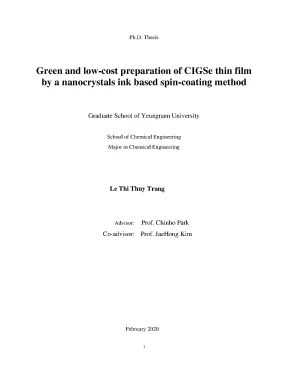
Tải xuống để đọc toàn bộThesis Green and low-cost preparation of CIGSe thin film by a nanocrystals ink based spin-coating method Graduate School of Yeungnam University School of Chemical Engineering Major in Chemical Engineering Le Thi Thuy Trang Advisor: Prof. Chinho Park Co-advisor: Prof. JaeHong Kim February 2020 i Ph. Thesis Green and low-cost preparation of CIGSe thin film by a nanocrystals ink based spin-coating method Advisor: Prof.
Chinho Park Co-advisor: Prof. JaeHong Kim Presented as Ph. Thesis February 2020 Graduate School of Yeungnam University School of Chemical Engineering Major in Chemical Engineering Le Thi Thuy Trang iii Acknowledgements I woud like to express my deep gratitude to my advisor, Professor Chinho Park at the School of chemical engineering. He has provided me the invaluable contributions in the research work by various profitable discussions.
His devoted instructions have been my sources of inspiration during Ph. periods, and have given me the great encouragement to fulfill both the research and writing of this thesis. I deeply thank to Professor JaeHong Kim, who has supported me to complete this Ph. My special thanks also go to Dr.
Vasu and Dr. Nguyen for their valuable comments and suggestions in my research. I am thankful to the IMSL lab’s members who have ever helped me many things. I will remember for their trust and friendship.
Your sentiments toward me are quite precious. I thank to my family for giving me a wider perspective on things, unlimited forbearance, and the time deprived from them. Last, I gratefully acknowledge Yeungnam university and BK 21 program because of their supports. December, 2019 Le Thi Thuy Trang iv Abstract This thesis presents our efforts that aim towards a green and low cost prodedure to fabricate CIGSe thin films which would be used as absorber layers for the thin film solar cell industry.
So, an ―ink‖ solution based process, using spin-coating technique, followed by annealing in selenium environment with different temperature programs was utilized to prepare CIGSe thin film. Firstly, CIGSe nanoparticles were synthesized using NaBH4 containing green solvent – ethanol by a sonochemical method. The effect of the ultrasonification time intervals on the synthesis was investigated in the range of 2-5 hr, 5 hr was found to be the most suitable time to obtain the expected CuIn0. The as-synthesized CIGSe nanoparticles possessed a tetragonal structure with quasi-spherical shape, and the targeted Cu(In0.
A new reaction scheme is proposed to explain the role of NaBH4 in the plausible reaction paths. The non-toxic solvent used in the synthesis with no additional heating makes the developed method cheaper and ―greener‖ than the previously reported methods. Next, three different solvents: 2-propanol, 2-methoxyethanol, and their 2:1 mixture (v/v ratio) were investigated as a dispersion medium for the as-synthesized CIGSe nanocrystals to form a stable ink solution. The last one – mixture of 2-propanol : 2-methoxyethanol = 2 : 1 (v/v) – was found to be the most suitable.
Furthermore, the influences of various annealing modes on the CIGSe grain size and density in the resulting film were also studied. The as-prepared CIGSe thin film was around 1 µm thick, possessed a tetragonal structure, and the band gap energy was estimated about ~ 1. The newly developed cheaper and ―greener‖ non-vacuum process was applied successfully from the nanocrystals synthesis to the formation of ―ink‖ solution, and produced v high quality thin films, which opens a new route to the cost-competitive commercialization of CIGSe thin film solar cells. vi Contents Acknowledgements.
v List of figures. viii Chapter 1: Literature Overview. The material system of Cu(In,Ga)Se2 quaternary. Introduction of the structural property.
Optical and electrical properties. Overview of solar cell. The story of solar cell. The operating principle of solar cell.
Thin film deposition techniques. The vacuum method. Chemical vapor deposition (CVD). The non-vacuum method.
The nanoparticles based method. Direct solution based process. Physical methods for characterizing solids. 18 Chapter 2: Green and low-cost synthesis of CIGSe nanoparticles using ethanol as a solvent by a sonochemical method - a new approach.
Results and discussion. 34 Chapter 3: The formation of CIGSe thin film by a nanocrystals ink based spin-coating method. Results and discussion. 57 List of puplications.
70 vii List of figures Chapter 1 Fig.1: The unit cell of the chalcopyrite lattice structure a) CuInSe2, b) Cu(In,Ga)Se2.2: The working of a silicon solar cell.3: The structure of a dye sensitized solar cells.4: Mechanism of dye sensitized solar cell.5: Basic structure or Organic Solar Cell. 1 6: The operating principle of solar cell. 1 7: Schematic of evaporation system. 1 8: Schematic illustration of different coevaporation recipes .9: Schematic of sputtering system .10: Schematic of chemical vapor deposition system .11: Schematic illustration of X-ray generation system.
1 12: (a) Section through an X-ray tube. (b) An X-ray emission spectrum.13: Basic components of a monochromatic XPS system .14: Schematic illustration of a raman spectroscopy system.15: Schematic illustration of scanning electron microscopy system.16: Schematic illustration of Scanning electron microscopy system.17: Block diagram of DTA.18: Schematic illustration of differential scanning calorimetry system. 30 viii Chapter 2 Fig.1: XRD patterns of the CIGSe nanoparticles synthesized with difference ultrasonification time.2: SEM images of CIGSe NPs with ultrasonification time of 2 hr (a), 3.3: Raman spectra of as-prepared CuIn0.3Se2 NPs with ultrasonification time of 5 hr.4: a) XPS survey spectrum and Cu 2p (b), In 3d (c), Ga 2p (d) , and Se 3d (e ) core-level spectrum of as-synthesized CuIn0.5: TEM images of CIGSe nanoparticles with ultrasonification time of 5 hr before (a) and after (b) annealed at 500 oC.6: XRD pattern of CuIn0.3Se2 NPs before and after annealed at 500 oC .7: Absorption spectrum (a) and plot of (αhν)2 versus photon energy hν (b) of the annealed CuIn0.1: The images of colloidal solutions with different dispersion mediums: 2-propanol (a), 2- methoxyethanol (b) and solvent mixture of 2-propanol and 2-methoxyethanol (c) after being kept in 1 month. 3 2: The images of the spin coated films by 2-propanol solvent based ink solution (a), and solvent mixture based ink solution (b).
3 3: Cross-section SEM image of CIGSe thin film with the first annealing mode. 3 4: Cross-section SEM image of CIGSe thin film with the second annealing mode. 3 5: Cross-section SEM image of CIGSe thin film with the third annealing mode. 3 6: Surface SEM image of CIGSe thin film with the third annealing mode.
3 7: XRD pattern of CIGSe thin film after being annealed with the third annealing mode.8: Plot of (αhν)2 versus photon energy hν of CIGSe thin film after being annealed with the third annealing mode. 55 x Chapter 1: Literature Overview 1. The material system of Cu(In,Ga)Se2 quaternary CuInxGa1-xSe2 (CIGSe) quaternary is a p-type semiconductor material which is a member of the I-III-VI2 chalcopyrites family [1]. It has been known as an effective light-absorbing layer for thin film solar cell industry, and CIGSe thin film solar cells were first studied at the Bell laboratories in 1975.
Much efforts have been done on CICSe solar cells, therefore the efficiency of CIGSe solar cells have reached up to 23. Introduction of the structural property. The basis for the structure of CIGSe quaternary is the structure of CISe ternary. Some indium atoms in unit cell of CISe ternary are replaced by gallium atoms to form unit cell of CIGSe [1].1: The unit cell of the chalcopyrite lattice structure a) CuInSe2, b) Cu(In,Ga)Se2 [3].
CIGSe crystals have the tetragonal chalcopyrite lattice structure which drived from the cubic structure of the group IV semiconductor. The unit cell is corresponds to two stacked zincblende unit cells, where copper, indium and gallium atoms are regularly ordered. The lattice parameters of CuInxGa1-xSe2 are a=b= 5.696, value of c depend on value x composition of Ga element [4]. Optical and electrical properties Optical properties CIGSe semiconductors possess high optical absorbtion coefficient α > 105 cm-1, and relatively low direct band gap energy value in the range 1.7 eV, resulting from the hybridization of Cu d-orbitals and Se p-orbitals in the valence bands [5,6].
The band gap energy of CuIn1-xGaxSe2 compounds depend on the Ga/Ga+In concentration ratio, but also by the Cu content. The optical band gap energy of CuInSe2 is about 1. when In atoms are gradually substituted by gallium atoms, the band gap can be increase to 1.68 eV, which is the optical band gap energy of CuGaSe2 [1]. The band gap energies of the CuIn1-xGaxSe2 quaternary with different compositions from x= 0 to 1 are calculated based on an empirical ―bowing equation‖ [7,8]: Eg= 1.167x(1-x) (1) Where the so-called optical bowing coefficient is 0.
Electrical properties The CuIn1-xGaxSe2 absorber layer is a p-type semiconductor with hole concentration about 1016 - 1018 cm-3 at room temperature. The hole mobilities have been obtained values in the range of 15-150 cm2/Vs with single crystals and values of 5-50 cm2/Vs with polycrystalline films [9,10]. Overview of solar cell 1. The story of solar cell 2 In 1839, a French physicist-Alexander Edmond Becquerel discovered the technology directly producing electricity from the solar energy [11].
This was the beginning of the solar cell technology-which open a new gate for the renewable energy technology. Solar cells are often divided into three main caregories which are called generations up to recent years: - The first generation: Monocrystalline silicon (mono c-Si), polycrystalline silicon (poly c-Si) and armophous silicon cells. - The second generation: amorphous silicon (a-Si), CdTe and CuInS/CIGS. - The third generation: DSSCs, Perovskite and organic The first generation The first silicon solar cell with an efficiency of 6% was studied at Bell laboratories and reported by Chapin, Fuller and Pearson in 1954 [12].
One year later, the first commercial solar cells with 2% efficient were produced by Hoffman Electronics corporation using wafers of silicon (monocrystalline silicon). The following success of this technology was mostly founded on the further development of the Czochalski method in the 1940s enabling the production of high purity silicon [13], leading to the efficiency of these solar cells currently reaching to 26. However, the cost of fabricating monocrystalline silicon solar cells are high because of the purification process of bulk. Mandelkorn created n-on-p silicon solar cells which were better suited for space with more resistance to radiation damage at U.
Signal Corps Laboratories, and these cells were applied to a space satellite ― Vanguard 1‖ – a first solar powered satellite launched at this year with a 0.1W, 100 cm2 solar panel [15]. 3 Different from monocrystalline silicon solar cells, the solar cells made from polycrystalline silicon or amorphous silicon are much cheaper because they are much less pure than monocrystalline silicon, therefore the way slicon made is easier and simpler. However, the highest efficient solar cell made from polycrystalline silicon is recorded of 22.3% [14], lower monocrystalline solar cell.2 shows structure of a silicon solar cell. A silicon solar cell typically is a sandwich of two layers : the first layer is a positive layer ( p-type silicon ) which usually made by doping silicon with boron to form extra holes in the lattice.
The second layer is a negative layer ( n-type silicon ) which usually made by doping silicon with phosphorus to gain extra electrons in the lattice.2: The working of a silicon solar cell [16]. Some limitations of this generation : Silicon possesses an indirect band gap with a low absorption coefficient, so it is not a ideal material for a light conversion. Besides, the silicon absorber layers require a high purity and a thickness up to around 200 µm, therefore the cost of fabrication is high and the product is less visual aesthetic. The second generation 4 The second generation solar cells were studied with the purpose of reducing limitations of the first generation solar cells mentioned above.
The advantage of this generation is that Semiconductor materials used in this generation possess direct band gap.
Nội dung được bảo vệ bản quyền — Tải xuống đầy đủ
Trích dẫn luận án này
Le Thi Thuy Trang (2020). Luận án tiến sĩ kỹ thuật hóa học green and low cost preparat [Luận án tiến sĩ, Yeungnam University]. LuanAn.net. https://luanan.net/hoa-hoc/method
Câu hỏi thường gặp
Luận án "Luận án tiến sĩ kỹ thuật hóa học green and low cost preparat" nghiên cứu về vấn đề gì?
Tài liệu: Luận án tiến sĩ kỹ thuật hóa học green and low cost preparation of cigse thin film by a nanocrystals ink based spin coating method. Tải miễn phí tại T
Luận án "Luận án tiến sĩ kỹ thuật hóa học green and low cost preparat" được bảo vệ tại trường nào?
Luận án này được bảo vệ tại Yeungnam University. Năm bảo vệ: 2020.
Luận án "Luận án tiến sĩ kỹ thuật hóa học green and low cost preparat" thuộc chuyên ngành gì?
Luận án "Luận án tiến sĩ kỹ thuật hóa học green and low cost preparat" thuộc chuyên ngành Chemical Engineering. Danh mục: Hóa Học.
Luận án "Luận án tiến sĩ kỹ thuật hóa học green and low cost preparat" có bao nhiêu trang?
Luận án "Luận án tiến sĩ kỹ thuật hóa học green and low cost preparat" có 81 trang. Bạn có thể xem trước một phần tài liệu ngay trên trang web trước khi tải về.
Cách tải luận án "Luận án tiến sĩ kỹ thuật hóa học green and low cost preparat" về máy như thế nào?
Để tải luận án về máy, bạn nhấn nút "Tải xuống ngay" trên trang này, sau đó hoàn tất thanh toán phí lưu trữ. File sẽ được tải xuống ngay sau khi thanh toán thành công. Hỗ trợ qua Zalo: 0559 297 239.