Tăng băng thông ngoại vi và giảm thiểu dark silicon với Chân cắm có thể chuyển đổi - Shaoming Chen
Tối ưu hiệu năng chip: Mở rộng băng thông ngoại vi, giảm thiểu dark silicon. Tăng tốc xử lý, tiết kiệm năng lượng cho các ứng dụng hiệu năng cao.
Năm xuất bản
Số trang
119
Thời gian đọc
18 phút
Lượt xem
1
Lượt tải
0
Phí lưu trữ
40 Point
Tổng quan nhanh
- Chủ đề:
- 1. Tối ưu Băng thông Ngoại vi và Giảm Dark Silicon
- Số trang:
- 119 trang
- Trường:
- Louisiana State University and Agricultural and Mechanical College
- Chuyên ngành:
- Electrical and Computer Engineering
- Tác giả:
- Shaoming Chen
- Năm:
- 2016
Tóm tắt nội dung luận án
I. Tối ưu Băng thông Ngoại vi và Giảm Dark Silicon
Nghiên cứu này tập trung vào hai thách thức chính trong kiến trúc chip hiện đại: hạn chế băng thông ngoại vi và sự xuất hiện của dark silicon. Các bộ xử lý đa lõi ngày càng đòi hỏi giao tiếp nhanh hơn với bộ nhớ và các thiết bị ngoại vi. Tuy nhiên, số lượng chân (pin) trên chip có giới hạn vật lý. Hạn chế này gây ra tắc nghẽn bus hệ thống, làm giảm hiệu suất tổng thể. Dark silicon là hiện tượng các vùng lớn trên chip phải tắt nguồn để quản lý nhiệt hoặc tiết kiệm năng lượng, ngay cả khi cần thiết cho tính toán. Các công nghệ giao diện I/O tốc độ cao mới như PCIe Gen 5, PCIe Gen 6, NVMe, USB4, và Thunderbolt đang phát triển, nhưng chúng vẫn đối mặt với các giới hạn vật lý của chân. Giải pháp ghim có thể chuyển đổi được đề xuất để giải quyết đồng thời cả hai vấn đề này. Công nghệ này mang lại khả năng cấu hình lại động các chân chip.
1.1. Thách thức băng thông và silicon tối
Băng thông ngoại vi là nút cổ chai lớn. Các bộ xử lý đa lõi hiện nay cần lượng lớn dữ liệu. Tốc độ truyền dữ liệu bị hạn chế bởi số chân và tần suất hoạt động. Dark silicon là phần chip không thể hoạt động do giới hạn năng lượng. Hiện tượng này ảnh hưởng đến hiệu suất tiềm năng của chip.
1.2. Giải pháp ghim có thể chuyển đổi
Ghim có thể chuyển đổi mang lại tính linh hoạt. Chúng cho phép thay đổi chức năng chân chip theo thời gian thực. Điều này giúp tối ưu hóa việc sử dụng tài nguyên chip. Giải pháp này hỗ trợ cả tăng băng thông và giảm tiêu thụ điện năng chip.
II. Công nghệ Ghim Có Thể Chuyển Đổi Hiệu Quả
Công nghệ ghim có thể chuyển đổi là một phương pháp cải tiến kiến trúc phần cứng. Nó cho phép các chân I/O trên chip thay đổi vai trò hoặc chế độ hoạt động một cách linh hoạt. Các chân có thể chuyển đổi giữa các chế độ bus khác nhau. Chế độ bus rộng sử dụng nhiều chân hơn để tăng tốc độ truyền dữ liệu. Chế độ liên kết đơn hoặc đa liên kết tối ưu hóa cho các tình huống khác nhau. Việc chuyển đổi này dựa trên các yêu cầu của ứng dụng hoặc khối lượng công việc. Công nghệ này có thể áp dụng cho nhiều loại giao diện. Các giao diện như PCIe Gen 5 và PCIe Gen 6 có thể hưởng lợi. Các thiết bị như NVMe, USB4, và Thunderbolt cũng có thể được tối ưu hóa. Điều này mang lại hiệu suất cao hơn và quản lý năng lượng tốt hơn.
2.1. Cơ chế hoạt động của ghim
Ghim có thể chuyển đổi hoạt động dựa trên logic điều khiển. Logic này xác định cấu hình chân tốt nhất. Quyết định dựa trên pha chương trình và yêu cầu tải. Cơ chế này đảm bảo sử dụng tối ưu các chân. Nó thích ứng với các thay đổi trong nhu cầu băng thông.
2.2. Chế độ bus rộng và đa liên kết
Chế độ bus rộng tăng cường băng thông tức thì. Nó sử dụng nhiều chân hơn cho một luồng dữ liệu. Chế độ đa liên kết cho phép nhiều kênh độc lập. Mỗi kênh có thể hoạt động ở tốc độ truyền dữ liệu riêng. Sự linh hoạt này giảm tắc nghẽn bus hệ thống.
2.3. Quản lý năng lượng chip động
Ghim có thể chuyển đổi đóng góp vào quản lý năng lượng. Chế độ hoạt động ít băng thông có thể giảm số lượng chân hoạt động. Điều này giúp giảm tiêu thụ điện năng chip. Các vùng silicon tối có thể được bật hoặc tắt một cách linh hoạt.
III. Nâng Cao Tốc Độ Truyền Dữ liệu I O Với Ghim
Khả năng tăng tốc độ truyền dữ liệu là lợi ích cốt lõi của ghim có thể chuyển đổi. Bằng cách cho phép các chân I/O cấu hình lại thành bus rộng hơn, hệ thống có thể xử lý nhiều dữ liệu hơn trong cùng một chu kỳ. Điều này trực tiếp giải quyết vấn đề tắc nghẽn bus hệ thống. Các bộ xử lý đa lõi và ứng dụng bộ nhớ chuyên sâu đặc biệt hưởng lợi. Tốc độ truyền dữ liệu cao hơn là yếu tố then chốt cho hiệu suất. Các giao diện I/O tốc độ cao như PCIe Gen 5 và PCIe Gen 6 đạt được tiềm năng tối đa. Các thiết bị lưu trữ NVMe cũng có thể đạt được hiệu suất vượt trội. Công nghệ này cũng cải thiện độ trễ I/O. Các ứng dụng nhạy cảm với độ trễ sẽ thấy sự khác biệt đáng kể.
3.1. Tăng tốc độ truyền dữ liệu
Ghim có thể chuyển đổi cho phép mở rộng băng thông động. Điều này tạo ra kênh dữ liệu rộng hơn khi cần. Kết quả là tốc độ truyền dữ liệu giữa chip và bộ nhớ/thiết bị ngoại vi được cải thiện rõ rệt. Hiệu suất ứng dụng được nâng cao đáng kể.
3.2. Giảm độ trễ I O và tắc nghẽn bus
Việc giảm tắc nghẽn bus hệ thống là trọng tâm. Bằng cách tối ưu hóa đường dẫn dữ liệu, độ trễ I/O được giảm xuống. Dữ liệu đến đích nhanh hơn. Điều này đặc biệt quan trọng cho các khối lượng công việc đòi hỏi.
3.3. Tối ưu cho khối lượng công việc
Công nghệ ghim có thể chuyển đổi thích ứng với nhiều loại tải. Đối với khối lượng công việc yêu cầu bộ nhớ, băng thông sẽ được ưu tiên. Đối với các tác vụ chuyên sâu tính toán, có thể tối ưu hóa năng lượng. Tính linh hoạt này đảm bảo hiệu suất tốt nhất cho mọi tình huống.
IV. Giảm Thiểu Tiêu Thụ Điện Năng Chip và Dark Silicon
Một mục tiêu quan trọng khác của công nghệ ghim có thể chuyển đổi là giảm thiểu dark silicon và tiêu thụ điện năng chip. Trong các bộ xử lý hiện đại, một phần lớn diện tích chip phải tắt nguồn. Lý do là để tuân thủ giới hạn nhiệt hoặc ngân sách năng lượng. Hiện tượng dark silicon ngăn cản việc sử dụng đầy đủ tiềm năng của chip. Ghim có thể chuyển đổi cung cấp một cơ chế giải quyết vấn đề này. Chúng cho phép phân phối lại năng lượng động. Các chân không sử dụng cho băng thông có thể được dùng cho nguồn điện. Hoặc các chân có thể được đặt ở chế độ tiết kiệm năng lượng. Điều này giúp duy trì hoạt động nhiều vùng chip hơn. Đồng thời, nó kiểm soát tổng tiêu thụ điện năng.
4.1. Tiết kiệm năng lượng thông qua ghim
Khi băng thông ngoại vi không cần mức tối đa, số lượng chân hoạt động có thể giảm. Các chân không hoạt động có thể chuyển sang chế độ ngủ. Điều này trực tiếp giảm tiêu thụ điện năng chip. Nó cũng giúp kéo dài tuổi thọ của thiết bị.
4.2. Giảm vùng silicon tối
Bằng cách phân phối lại năng lượng, nhiều phần của chip có thể được cấp điện. Điều này làm giảm đáng kể các vùng silicon tối. Các tài nguyên tính toán có sẵn tăng lên. Hiệu suất tổng thể của bộ xử lý được cải thiện.
4.3. Phân phối điện năng hiệu quả
Mạng phân phối điện năng được tối ưu hóa. Ghim có thể chuyển đổi cho phép thay đổi cấu hình nguồn động. Điều này giúp đáp ứng nhu cầu năng lượng tức thì của từng thành phần chip. Việc quản lý điện năng hiệu quả hơn dẫn đến ít lãng phí hơn.
V. Cải Tiến Băng Thông Bộ Nhớ và Liên Socket
Ngoài việc tối ưu hóa băng thông chip-to-memory, công nghệ ghim có thể chuyển đổi còn mở rộng lợi ích sang bộ nhớ PCM (Phase Change Memory) và giao tiếp liên socket. Bộ nhớ PCM là một công nghệ bộ nhớ phi biến đổi có tiềm năng cao. Ghim có thể chuyển đổi cho phép tăng cường hiệu suất của bộ nhớ PCM. Chúng có thể cung cấp băng thông cao hơn cho các khối lượng công việc chuyên sâu về bộ nhớ. Điều này đặc biệt có lợi cho các ứng dụng đa luồng và đa chương trình. Bên cạnh đó, băng thông liên socket cũng được cải thiện đáng kể. Trong các hệ thống đa bộ xử lý, giao tiếp giữa các socket thường là một nút cổ chai. Ghim có thể chuyển đổi giúp tăng tốc độ truyền dữ liệu qua các liên kết như QPI. Điều này giúp giảm độ trễ I/O trong các hệ thống lớn.
5.1. Tăng cường với bộ nhớ PCM
Bộ nhớ PCM hưởng lợi từ băng thông động. Ghim có thể chuyển đổi cung cấp các đường dẫn dữ liệu rộng hơn. Điều này cho phép truy cập nhanh hơn vào dữ liệu trong PCM. Nó tối ưu hóa hiệu suất cho các ứng dụng sử dụng PCM.
5.2. Băng thông liên socket hiệu quả
Giao tiếp giữa các socket được cải thiện. Ghim cho phép cấu hình lại các kênh liên socket. Điều này tăng tốc độ truyền dữ liệu giữa các bộ xử lý. Giảm tắc nghẽn bus hệ thống ở cấp độ hệ thống.
5.3. Mở rộng giao diện I O tốc độ cao
Công nghệ này mở đường cho việc sử dụng rộng rãi hơn các giao diện I/O tốc độ cao. Các giao diện như PCIe Gen 5 và Gen 6 có thể được tận dụng tối đa. Việc này bao gồm cả kết nối NVMe, USB4, và Thunderbolt.
VI. Giao Diện I O Tốc Độ Cao Cho Tương Lai
Công nghệ ghim có thể chuyển đổi định hình tương lai của giao diện I/O tốc độ cao. Các chuẩn như PCIe Gen 5 và PCIe Gen 6 đang phát triển mạnh mẽ. Chúng đòi hỏi khả năng thích ứng cao từ phần cứng. Ghim có thể chuyển đổi cung cấp tính linh hoạt này. Chúng đảm bảo các hệ thống có thể tận dụng hoàn toàn băng thông tiềm năng của các chuẩn mới. Các ứng dụng như NVMe, USB4, và Thunderbolt sẽ thấy hiệu suất tăng đáng kể. Tốc độ truyền dữ liệu cao hơn sẽ thúc đẩy đổi mới trong lưu trữ, kết nối và xử lý dữ liệu. Độ trễ I/O thấp hơn là rất quan trọng cho các ứng dụng thời gian thực. Việc giảm thiểu dark silicon cũng góp phần tạo ra các chip mạnh mẽ hơn, hiệu quả hơn. Công nghệ này là một bước tiến quan trọng trong thiết kế chip và hệ thống.
6.1. Hỗ trợ PCIe Gen 5 và Gen 6
Ghim có thể chuyển đổi tối ưu hóa các giao diện PCIe. Chúng cho phép các thế hệ PCIe Gen 5 và PCIe Gen 6 đạt hiệu suất cao nhất. Điều này đảm bảo khả năng tương thích và nâng cấp trong tương lai.
6.2. Ứng dụng NVMe USB4 Thunderbolt
Các công nghệ này hưởng lợi từ băng thông linh hoạt. NVMe cho SSD, USB4 và Thunderbolt cho kết nối đa năng. Ghim có thể chuyển đổi mở khóa tiềm năng đầy đủ của chúng.
6.3. Triển vọng và thách thức công nghệ
Công nghệ này có triển vọng lớn cho các hệ thống máy tính. Tuy nhiên, việc triển khai cần sự chính xác trong thiết kế mạch. Quản lý chuyển đổi động là một thách thức. Nghiên cứu tiếp theo sẽ tập trung vào tối ưu hóa và tích hợp.
Mục lục chi tiết luận án
Tải xuống file đầy đủ để xem toàn bộ nội dung
Tải đầy đủ (119 trang)Trích đoạn nội dung luận án
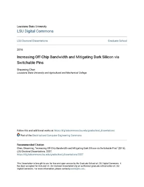
Tải xuống để đọc toàn bộLouisiana State University LSU Digital Commons LSU Doctoral Dissertations Graduate School 2016 Increasing Off-Chip Bandwidth and Mitigating Dark Silicon via Switchable Pins Shaoming Chen Louisiana State University and Agricultural and Mechanical College Follow this and additional works at: https://digitalcommons.edu/gradschool_dissertations Part of the Electrical and Computer Engineering Commons Recommended Citation Chen, Shaoming, "Increasing Off-Chip Bandwidth and Mitigating Dark Silicon via Switchable Pins" (2016). LSU Doctoral Dissertations.edu/gradschool_dissertations/3337 This Dissertation is brought to you for free and open access by the Graduate School at LSU Digital Commons. It has been accepted for inclusion in LSU Doctoral Dissertations by an authorized graduate school editor of LSU Digital Commons. For more information, please contactgradetd@lsu.
INCREASING OFF-CHIP BANDWIDTH AND MITIGATING DARK SILICON VIA SWITCHABLE PINS A Dissertation Submitted to the Graduate Faculty of the Louisiana State University and Agricultural and Mechanical College in partial fulfillment of the requirements for the degree of Doctor of Philosophy in School of Electrical Engineering and Computer Science by Shaoming Chen B., Huazhong University of Science and Technology, Wuhan, China 2008 M., Huazhong University of Science and Technology, Wuhan, China 2011 August 2016 ACKNOWLEDGEMENTS I would like to dedicate the dissertation to my parents and my friends for their continuous support and encouragement throughout my entire life. This dissertation is completed with the valuable help and support from a lot of people including my advisor, Dr. He thoughtfully guided me to pick up the emerging topic and offered valuable advises for my study. Ashok Srivastava gave appreciated help of circuit design and encouraged me to response bitter feedbacks from reviewers.
Bin Li from Department of Experimental Statistics provided insightful statistical methods to help me to analyze experimental data. David Koppelman and Dr. Rudy Hirschheim as my committee members take their valuable time to supervise my dissertation and attend my defense. I sincerely appreciate the professors’ supports as the foundation of the work.
I also would like to thanks my co-workers in my lab. Zhang provided insight thoughts that helped me to develop the dissertation. Yue devoted enormous effort on circuit design especially on power delivery network. Zhou elaborated the circuit design and helped me to improve the circuit design.
Sam proofread the work and gave me wonderful feedbacks. I am thankful to the Department of Electrical and Computer Engineering for providing assistantship throughout my study. Finally, I would like thank all the friends I met at LSU for making my life here wonderful and memorable. ii TABLE OF CONTENTS ACKNOWLEDGEMENTS.
ii LIST OF TABLES. v LIST OF FIGURES. 6 INCREASING OFF-CHIP BANDWIDTH IN MULTI-CORE PROCESSORS WITH SWITCHABLE PINS. 9 Off-Chip Bus Connection.
16 Power Delivery Simulation. 18 Runtime Switch Conditions. 25 Performance and Energy Efficiency Metrics. 27 Memory-Intensive Workloads.
28 Wide-bus mode. 35 Compute-Intensive Workloads. 38 MITIGATING DARK SILICON VIA SWITCHABLE PINS. 43 Power Delivery Network.
50 Dynamic Pin Switching based on Program Phases. 56 Dim Silicon Result. 60 BOOSTING OFF-CHIP BANDWIDTH WITH PCM VIA SWITCHABLE PINS. 64 Memory-Intensive Multi-threaded Workloads.
64 Memory-Intensive Multi-programmed Workloads using PCM. 65 Memory-Intensive Multi-threaded Workloads using PCM. 66 Mixed Multi-program Workloads on the memory subsystem using PCM. 68 INCREASING INTER-SOCKET BANDWIDTH VIA SWITCHABLE PINS.
72 Off-chip connection. 80 Area Overhead & Propagation Delay. 86 Performance of the static switching. 86 Performance of the dynamical switching.
89 Enhancement from a stride prefetcher. 90 The bandwidth of the DRAM cache. 92 The size of DRAM cache. 93 The frequency of QPI buses.
107 iv LIST OF TABLES Table 2-1. Pin allocation of an Intel Processor i5-4670. Power network model parameters. Processor power and frequency parameters for different number of buses.
The Configuration of the simulated system. The selected memory-intensive and compute-intensive workloads. Pin allocation of the Intel Xeon Processor E5-2450L. Processor configurations under different cooling techniques.
Parameters of the performance and power models. Simulated multi-program workloads. Benchmark memory statistics. The configuration of the simulated system.
The selected workloads. The intervals in the multi-link mode and in the single-link mode as well as the times of switching to the multi-link mode and the single-link mode. 89 v LIST OF FIGURES Figure 1-1. Normalized weighted speedup and off-chip bandwidth of 4 lbm co-running on a processor with 1,2,3,4 memory channels.
Power and memory bandwidth (8 copies of DEALII from SPEC2006). The latency breakdown of un-core requests in the simulated system with two sockets. The circuit of pin switch. The overview of the hardware design of off-chip bus connection for switching between the Multi-bus mode and the Single-bus mode.
The Overview of the hardware design of memory controller for switching between the Multi-bus mode and the Single-bus mode. Spice models for signal integrity simulation. The eye diagrams. RLC power delivery model.
The normalized off-chip latencies and on-chip latencies of workloads against the total execution time. The normalized weighted speedup of memory-intensive workloads with 2, 3, and 4 buses against the each baseline. The average normalized weighted speedup of memory workloads in geometric mean with multi-bus mode. Each normalize to the same configuration with single bus mode.
The normalized weighted speedup of memory intensive workloads boosted by Static Switching and Dynamic Switching with 3 buses against the baseline. The increased bandwidth due to pin switching. The normalized bandwidth of baseline, static pin switching, and dynamic pin switching. The improved throughput of Dynamic Switching boosted by a stride prefetchers (degree = 1, 2, 4) for memory-Intensive workloads.
The off-chip bandwidth of Dynamic Switching improved by a stride prefetcher (degree = 1, 2, 4) for memory-Intensive workloads. The performance of memory intensive workloads for the baseline (core frequency of 4GHz and a memory bus of 64 bits) and two configurations of wide bus vi mode (core frequency of 3.6GHz and a memory bus of 128 bits; core frequency of 2.8GHz and a memory bus of 256 bits). The off-chip bandwidth of memory intensive workloads for the baseline (core frequency of 4GHz and a memory bus of 64 bits) and two configurations of wide bus mode (core frequency of 3.6GHz and a memory bus of 128 bits, core frequency of 2.8GHz and a memory bus of 256 bits). The normalized EPI of Dynamic Switching for memory intensive workloads with 3 buses, and the EPI from DVFS (running on 2.4GHz with the single bus).
The normalized weighted speedup of mixed workloads boosted by Static Switching and Dynamic Switching. The improved throughput of Dynamic Switching boosted by a stride prefetchers (degree = 1, 2, 4) for mixed workloads. The normalized weighted speedup of Compute-Intensive workloads with Static Switching and Dynamic Switching. Structure of a packaged chip (8 copies of DEALII from SPEC2006).
Design overview on the proposed scheme. Layout of wrapped around large transistor. Circuits when a switchable pin is used for signal transmission. Received eye diagram.
Workflow of dynamic switching. Floorplan of the chip multiprocessor. Performance speedup when the processor is in dim silicon mode. Number of L2 cache misses per 1K instructions on a processor configured to 8×2.
Prediction accuracy on a processor in dim silicon mode. Performance evaluation of multi-threaded workloads with Dynamic Switching and prefetching (degree = 1, 4). Normalized consumption of off-chip bandwidth of multi-threaded workloads using Dynamic Switching and prefetching (degree = 1, 4). Improved throughput of Dynamic Switching boosted by stride prefetchers (degree = 1, 2, 4) for memory-Intensive workloads using PCM.
Normalized off-chip bandwidth of Dynamic Switching boosted by stride prefetchers (degree = 1, 2, 4) for memory-Intensive workloads using PCM. Performance evaluation of multi-threaded workloads using Dynamic Switching and prefetching (degree=1, 4) on the PCM subsystem. Normalized consumed off-chip bandwidth of multi-threaded workloads using Dynamic Switching and prefetching (degree =1, 4) on the PCM subsystem. The improved throughput of Dynamic Switching boosted by stride prefetchers (degree = 1, 4) for mixed workloads with PCM.
The simulated system running in the single-link mode and the multi-link mode. The off-chip bus connection in the single-link mode and the multi-link mode. The memory controller running in the single-link mode and the multi-link mode. The physical layers of QPI running in the single-link mode and the multi-link mode.
The Spice models for QPI buses and memory buses in single-link mode and the multi-link mode. The normalized speedup of the static switching and the dynamic switching compared with the baseline. The latency of un-core requests for the static switching normalized against that of the baseline. The normalized speedup of the static switching and the dynamic switching compared with baseline for the workloads with moderate or low inter-socket traffic.
The energy consumption in the static switching normalized against the baseline. The normalized speedup of the static switching with a prefetcher (degree 1, 2, 4) compared with baseline and the prefetcher. The ratio between the un-core latencies of QPI and the total un-core latencies with the baseline and a prefetcher (degree 1, 2, 4). The normalized speedup of the static switching with the different bandwidths of DRAM cache.
The normalized speedup of the static switching with the different sizes of DRAM cache. The normalized latencies of un-core requests in the static switching with the different sizes of DRAM cache. The normalized speedup of the static switching with the different frequencies of QPI. The ratio between the un-core latencies of QPI and the total un-core latencies with the baseline and the different frequencies of QPI buses.
96 ix ABSTRACT Off-chip memory bandwidth has been considered as one of the major limiting factors to processor performance, especially for multi-cores and many-cores. Conventional processor design allocates a large portion of off-chip pins to deliver power, leaving a small number of pins for processor signal communication. We observed that the processor requires much less power than that can be supplied during memory intensive stages in some cases. In this work, we propose a dynamic pin switch technique to alleviate the bandwidth limitation issue.
The technique is introduced to dynamically exploit the surplus pins for power delivery in the memory intensive phases and uses them to provide extra bandwidth for the program executions, thus significantly boosting the performance. We also explore its performance benefit in the era of Phase-change memory (PCM) and prove that the technique can be applied beyond DRAM-based memory systems. On the other hand, the end of Dennard Scaling has led to a large amount of inactive or significantly under-clocked transistors on modern chip multi-processors in order to comply with the power budget and prevent the processors from overheating. This so-called “dark silicon” is one of the most critical constraints that will hinder the scaling with Moore’s Law in the future.
While advanced cooling techniques, such as liquid cooling, can effectively decrease the chip temperature and alleviate the power constraints; the peak performance, determined by the maximum number of transistors which are allowed to switch simultaneously, is still confined by the amount of power pins on the chip package. In this paper, we propose a novel mechanism to power up the dark silicon by dynamically switching a portion of I/O pins to power pins when off-chip x communications are less frequent. By enabling extra cores or increasing processor frequency, the proposed strategy can significantly boost performance compared with traditional designs. Using the switchable pins can increase inter-socket bandwidth as one of performance bottlenecks.
Multi-socket computer systems are popular in workstations and servers. However, they suffer from the relatively low bandwidth of inter-socket communication especially for massive parallel workloads that generates many inter-socket requests for synchronizations and remote memory accesses. The inter-socket traffic poses a huge pressure on the underlying networks fully connecting all processors with the limited bandwidth that is confined by pin resources.
Nội dung được bảo vệ bản quyền — Tải xuống đầy đủ
Trích dẫn luận án này
Shaoming Chen (2016). Tăng băng thông ngoại vi và giảm thiểu dark silicon [Luận án tiến sĩ, Louisiana State University and Agricultural and Mechanical College]. LuanAn.net. https://luanan.net/cong-nghe-thong-tin/tang-bang-thong-ngoai-vi-giam-thieu-dark-silicon-chan-cam-chuyen-doi
Câu hỏi thường gặp
Luận án "Tăng băng thông ngoại vi và giảm thiểu dark silicon" nghiên cứu về vấn đề gì?
Tối ưu hiệu năng chip: Mở rộng băng thông ngoại vi, giảm thiểu dark silicon. Tăng tốc xử lý, tiết kiệm năng lượng cho các ứng dụng hiệu năng cao.
Luận án "Tăng băng thông ngoại vi và giảm thiểu dark silicon" được bảo vệ tại trường nào?
Luận án này được bảo vệ tại Louisiana State University and Agricultural and Mechanical College. Năm bảo vệ: 2016.
Luận án "Tăng băng thông ngoại vi và giảm thiểu dark silicon" thuộc chuyên ngành gì?
Luận án "Tăng băng thông ngoại vi và giảm thiểu dark silicon" thuộc chuyên ngành Electrical and Computer Engineering. Danh mục: Công Nghệ Thông Tin.
Luận án "Tăng băng thông ngoại vi và giảm thiểu dark silicon" có bao nhiêu trang?
Luận án "Tăng băng thông ngoại vi và giảm thiểu dark silicon" có 119 trang. Bạn có thể xem trước một phần tài liệu ngay trên trang web trước khi tải về.
Cách tải luận án "Tăng băng thông ngoại vi và giảm thiểu dark silicon" về máy như thế nào?
Để tải luận án về máy, bạn nhấn nút "Tải xuống ngay" trên trang này, sau đó hoàn tất thanh toán phí lưu trữ. File sẽ được tải xuống ngay sau khi thanh toán thành công. Hỗ trợ qua Zalo: 0559 297 239.